Current Research Interests
High-Linearity Operational Transconductance Amplifier
(OTA)
The
operational transconductance amplifier (OTA), or transconductor, is one
of the
most important building blocks in analog circuits. The transconductor
can be
used for voltage-controlled oscillator (VCO), Gm-C filter,
continuous-time
sigma-delta modulator, and multiplier. In modern nanometer technology,
short
channel effects will degrade the ideal square law equation of the
saturation–region operation, affect the linearity performance of the
transconductor, and thus more suitable solutions should be investigated.
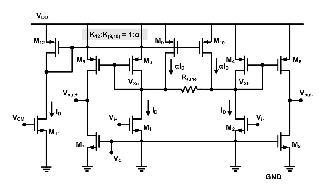
The transconductor linearity is best enhanced with different
operation
regions of the MOS device, especially when operating from a low supply.
The
MOSFETs working in different operation regions with suitable parameters
have
been used to achieve the cancellation of second order terms of the
transconductance for high linearity. Also, by using two cross coupling
pseudo-differential pairs and the source degeneration structure, the
nonlinearity caused by short channel effect from small feature size can
be
minimized. The short channel effect was compensated and minimized for
several
different architectures with high linearity performance under low
supply
voltage. The speed of the transconductors has also been enhanced while
still
maintaining its excellent linearity performance.
Wide Tuning Range Continuous-Time Gm-C Filter
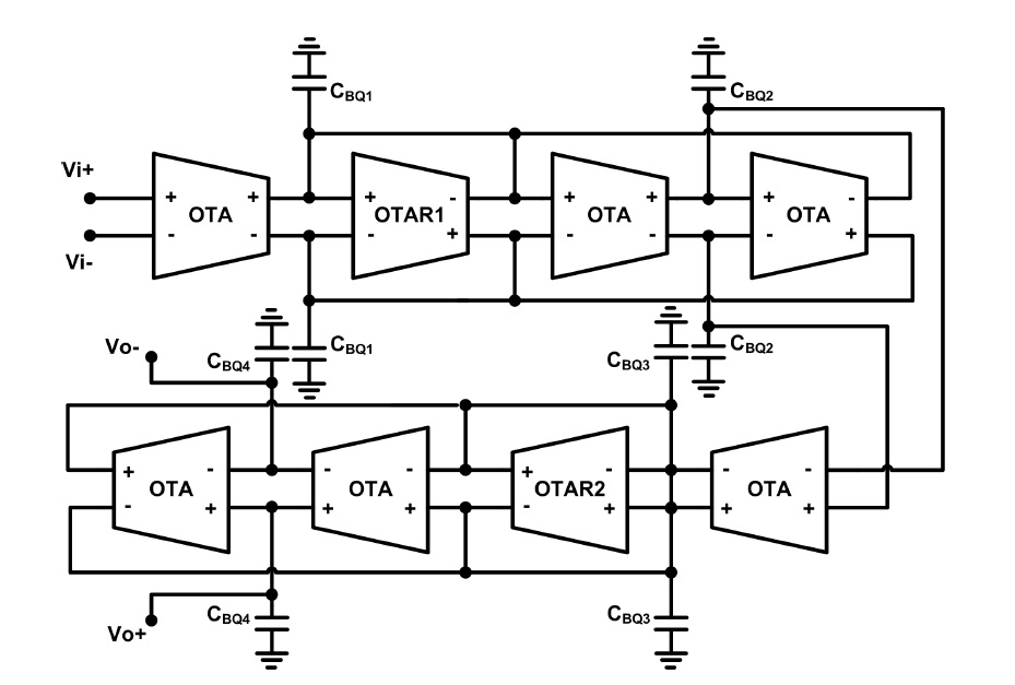
The continuous-time Gm-C filters have been
widely used in various high
speed applications, such as high data-rate read channel hard disks,
wireline
and wireless communications. For wireless communication application,
recent
demand for multi-standard transceivers calls for adopting
direct-conversion
architectures to achieve the highest level of integration and for ease
of
system design. However, an array or a stack of channel selection
filters in a
multi-standard radio design may not be power-efficient and would need
large
chip areas. Therefore, there is a strong motivation to realize a single
baseband channel select filter such that it meets the requirements of
multi-mode
applications.
Several multi-mode channel selection
filters under advanced CMOS process
have been proposed for the system-on-a-chip strategy, based on the
high-performance transconductors. The circuit design not only combines
several
standards in a wireless communication system, but also reduces the
required
chip area. The filter designs with low supply voltage introduces a very
wide
tuning range channel selection filter compared with previous works. Besides, a 1GHz 4th-order equiripple
linear-phase Gm-C low-pass filter, exhibiting the widest bandwidth
reported in
0.18um CMOS process, has also been proposed. A high speed OTA based on
the
inverter structure is realized. Transconductance tuning can be achieved
by
adjusting the bulk voltage using the Deep-NWELL technology. The
automatic
tuning circuit was also designed to compensate for the process and
temperature
variation and relaxes the speed requirement of the tuning blocks.
Low-Spur Frequency Synthesizer/Phase-Locked Loop
Phase-locked loops (PLLs) are widely used to
generate high-accuracy
clocks on chip. A clock with high spectral purity is required in many
applications, such as in communication systems to up-convert and
down-convert
the wanted signals, and in analog-to-digital converts (ADCs) to
accurately
define the sampling moments. One of the major sources of noise reducing
the
spurious-free dynamic range (SFDR) is the switching noise from the
charge pump
(CP) at the reference frequency. The switching noise modulates the
control
voltage and hence the output frequency of the voltage-controlled
oscillator
(VCO). Two tones that reduce the system performance appears at the
upper and
lower sidebands around the carrier. A narrow loop bandwidth can be used
to
suppress the ripple, thereby reducing the VCO spur level. However, the
PLL
needs more locking time and a larger LPF area, which is difficult to
implement
in the SOC design. A large bandwidth can offer a fast locking time and
reduce
the on-chip filter area, but it also reduces the sensitivity of the VCO
output.
In order to alleviate the tradeoff between low
spur and large bandwidth,
several novel architectures has been proposed by exploiting randomly
selected
PFD, random pulsewidth matching (RPWM), and sub-sampling charge pump
(SSCP) to
achieve low-reference-spur PLLs. Multiple PFDs are utilized to be
randomly
selected so as to randomize the CP output ripples. The RPWM is used to
generate
the matched CP pulsewidth, and randomize and average the ripples on the
control
voltage of the VCO. An SSCP is also utilized to reduce ripples on the
control
voltage in order to achieve a low spur level and relatively smooth
spectrum.
Through the randomization and average of the pulsewidth and the
reduction of
current mismatch, the frequency synthesizer can reduce the ripples on
the
control voltage of the voltage-controlled oscillator in order to reduce
the
reference spur at the output of the phase-locked loop.
Power Management Integrated Circuit
Smart handheld devices are becoming
increasingly popular. Different
types of power management circuits are placed in handheld devices to
provide
system circuits with stable power supply. Integrated circuits, such as
multimedia, consumer electronics, processor chips, and SOCs, require
supplies
from power management circuits with various structures based on the
circuit
specifications of each sub-block. Several types of power management
circuits
have been proposed, including capacitor-less low-dropout (LDO)
regulators,
single-inductor multiple-output boost converters, dual-output
switched-capacitor
DC–DC converters, and so on.
An output-capacitorless LDO voltage regulator
that achieves fast
transient responses by hybrid dynamic biasing is proposed. The hybrid
dynamic
biasing in the proposed transient improvement circuit is activated
through
capacitive coupling. The proposed transient improvement circuit senses
the LDO
output change so as to increase the bias current instantly. A
freewheel-charge-pump-controlled (FCPC) design is introduced for a
single-inductor
multiple-output (SIMO) DC–DC converter. By applying the FCPC technique,
the
freewheel switching time is reused, and two extra charge-pump outputs
are
provided by time recycling, with no cost in time sequences. The
converter has
two step-up outputs and two charge-pump outputs that can be higher than
the
input supply. An inductorless dual-output switched-capacitor DC–DC
converter
employing pseudo-three-phase swap-and-cross control (PTPSCC) and an
amplitude
modulation mechanism (AMM) is presented. The AMM circuit scales the
amplitudes
of the driving signals for the switches according to the loading
conditions in
order to minimize switching losses. To reduce output ripples, average
charge
distribution, and improve load regulation, the PTPSCC circuit
continuously
switches power transistors to deliver enough charge to the outputs by
keeping
at least one flying capacitor connected to each output.
Wide-Bandwidth Continuous-Time Delta-Sigma Modulator
Recently, the demands for analog-to-digital
converters (ADCs) in
wireless standards, such as LTE-A, have increased, which has pushed ADC
bandwidth up to a few tens of megahertz (MHz) and resolution to more
than 10
bits. As compared with Nyquist rate ADCs, continuous-time delta-sigma
(CT-ΔΣ)
modulators are particularly suited in wireless receivers due to several
attractive features, like implicit anti-aliasing filter and resistive
input
impedance. Applying CT circuits in the loop filter can relax the speed
and
power requirements of the analog circuits in ΔΣ modulators, as compared
with
discrete-time (DT) counterparts. CT-ΔΣ modulators can also operate at
high speed
with low power consumption.
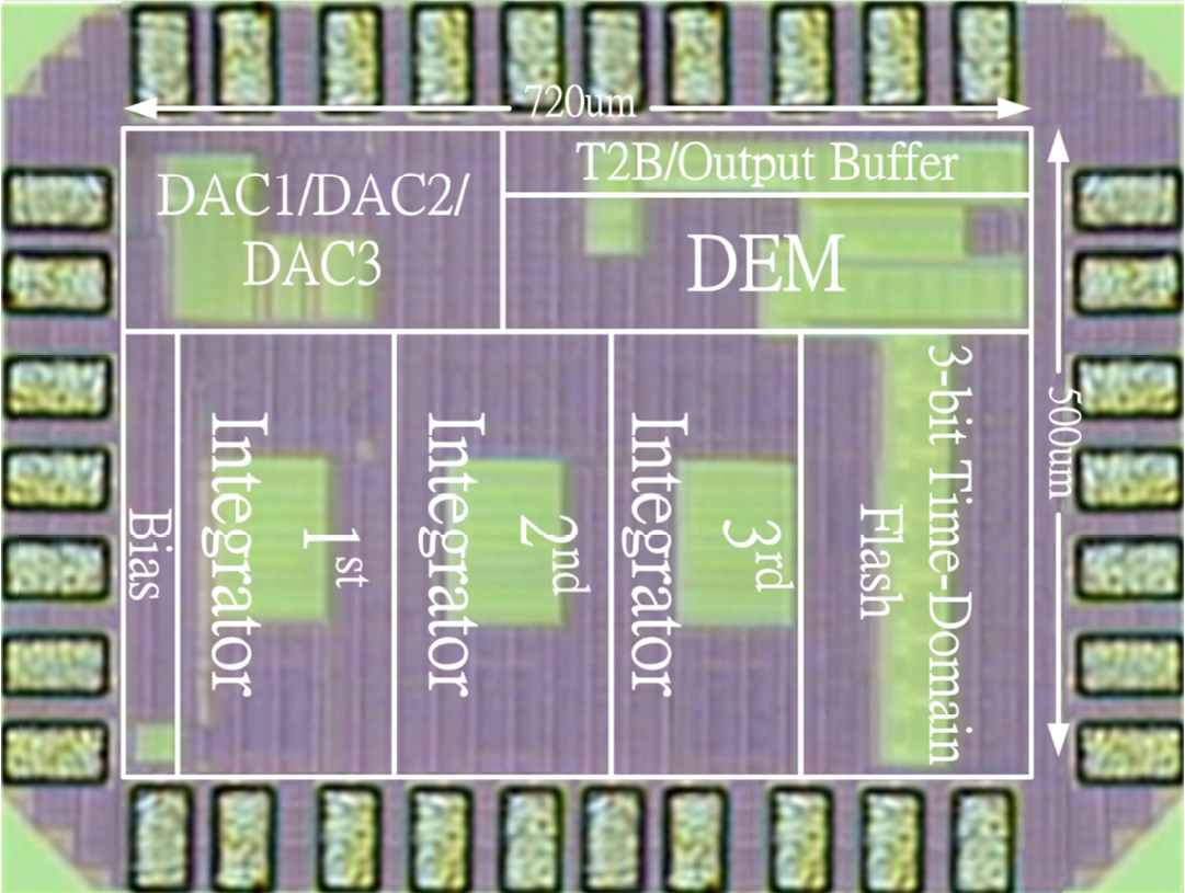
A power-efficient realization of a third-order
continuous-time
delta-sigma modulator with 3-bit time-domain flash quantizer (TDFQ) and
data-weighted averaging (DWA) based on the shifter output and input is
presented. Using the time-domain quantizer can overcome design issues
in low
voltage supply during CMOS downscaling. The CT-ΔΣ modulator uses the
proposed
TDFQ instead of a voltage-domain quantizer to reduce power consumption.
The
proposed TDFQ solves the linearity problem of the delay-based
voltage-to-time
converter (VTC) without calibration circuit while also increasing the
quantizer
input range and saving energy. Moreover, in order to reduce the
mismatch
effects of a multibit DAC and achieve low power consumption,
implementation of
a low-power DWA circuit is proposed without using a digital adder to
calculate pointer
for controlling barrel shift circuit.
Low-Glitch Current-Steering Digtal-to-Analog Converter
The Current-steering digital-to-analog
converter (DAC) is a good
candidate for high-speed DAC applications because it can drive low
impedance
directly with good linearity, and without needing high-speed buffers.
Current-steering DACs are based on an array of current sources that are
switched to the output which is connected with 50 ohm resistor, and the
differential architecture has often been used because even-orders
errors could
be eliminated. Unary and segmented DAC architectures need
binary-to-thermometer
decoders and delay cells, which increase circuit complexity and digital
power
consumption, so they come at cost (area, power, complexity, …) for
high-speed
and high-resolution DACs. Accounting for power consumption, chip size,
and
circuit complexity, the binary-weighted architecture is still a good
candidate
for medium-to-high resolution and sampling rate. It achieves both
static and
dynamic specifications at low cost.
A 10-bit high-speed and low-glitch pure
binary-weighted current-steering
DAC is proposed. In general, the largest glitch is generated during
major carry
transitions (011...1 à 100...0) because all bits are switched and
timing skews
exist among different current switches for binary-weighted DACs. The
proposed
converter uses variable-delay buffers to compensate for the delay
difference
among different bits, and to reduce glitch energy and improve
spurious-free
dynamic range (SFDR). The other method of reducing timing-skew among
different
bits is also proposed. The calculation method of dynamic capacitance
was used
to estimate the input capacitance of the current switches more
precisely, and
capacitance compensation was made for the input capacitance among
different
bits. Because the area of current-steering DAC is dominated by the size
of
current source arrays, a new architecture of current source arrays was
designed
to reduce the chip area without digital calibration. A new architecture
of
12-bit binary-weighted current-steering DAC with dual reference
currents is
presented. Instead of 4096 unit current cells required for conventional
12-bit
DAC, the proposed design uses only 192 unit current sources, and the
silicon
area of the generation circuit of two reference currents is very
compact as
well. The core area of the 12-bit DAC is almost the same as that of a
conventional 10-bit DAC. Besides, the output impedance of the unit
current-source transistor can be reduced to 1/32 that of the
conventional DAC.
This architecture has the advantages of compact area and low power.
Along with the demand from consumer
electronic products, portable devices
industries, and internet of things (IoT), temperature monitoring and
thermal
management systems have been developed rapidly, which can be used for
environment temperature monitoring, risk control of thermal damage, and
manufacture yield control. For these applications, the temperature
sensor is
one of the very important elements, especially that on-chip temperature
sensors
can gain the advantages of low fabrication cost, small dimension, low
power
dissipation, and elimination of the off-chip thermocouple.
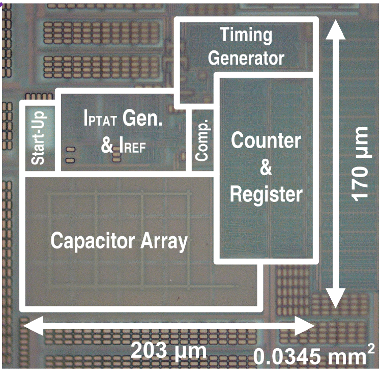
A current-mode dual-slope CMOS temperature
sensor is presented. It
employs a proportional-to-absolute-temperature (PTAT) current
generator, which
operates in the sub-threshold region, and a novel
temperature-insensitive CMOS
inverter, replacing a traditional voltage comparator for power saving,
to create
PTAT pulse width. A binary counter is then utilized to quantize the
pulse to a
digital output value. It achieves good temperature accuracy over the
common
industrial temperature range by utilizing second-order curvature
correction,
and great temperature resolution. The utilized dual-slope architecture
has the
advantages of compactness, power-saving, and high design flexibility.
High-Resolution Successive Approximation Register (SAR)
ADC
With the progress of the process technology,
SAR ADCs achieving lower
power dissipation can be applied to wide bandwidth system with medium
resolution. The primary sources of power consumption in SAR ADCs are
the
capacitive digital-to-analog converter (DAC), comparator, and SAR logic
control
circuit, among which the capacitive DAC dominates the overall power
dissipation. To improve the power dissipation, many techniques were
investigated by improving the power efficiency of the capacitive DAC.
The
Vcm-based charge recovery technique achieves 33.4% reduction in
switching
energy compared with the monotonic switching technique, whereas 50.1%
reduction
is achieved by the method of switchback switching. The split-capacitor
Vcm-based capacitor-switching scheme reduces the switching energy by
58.27%. A
high energy-efficient switching scheme is proposed. The proposed
switching
scheme reduces the energy dissipation by 75% compared with the
monotonic
switching technique. In addition, the total capacitance in the
capacitive DAC
is reduced by 50%.
At the resolution of 10 bits and beyond, the
precision of the SAR ADC is
limited by the accuracy of the comparator. There were many methods to
improve
the accuracy of the comparator, such as auto zeroing, offset storage,
and
digital cancellation. In our study, an offset calibration technique is
proposed
to enhance the resolution of the SAR ADC.